Henry Ott Consultants
Electromagnetic Compatibility Consulting and Training
Grounding of Mixed
Signal PCBs
A question that I hear often is: How do I prevent digital
logic ground currents from contaminating my low level analog
circuitry?
This is a good question without a simple answer. Most A/D
converter
manufacturer's data books and application notes provide little if any
useful
information on the subject. If they do provide information, it is
usually only applicable to a simple system containing only one A/D
converter.
Some people suggest splitting the ground plane in order to isolate
the
digital ground currents from the analog ground currents. Although
the split plane approach can be made to work, it has many potential
problems
especially in large complicated systems. Can you list some of
these
problems? One of the major ones is that you can not route a trace
over the split in the plane (see Tech Tip Slots
in Ground Planes). It is always better to have only a
single
reference plane for a system.
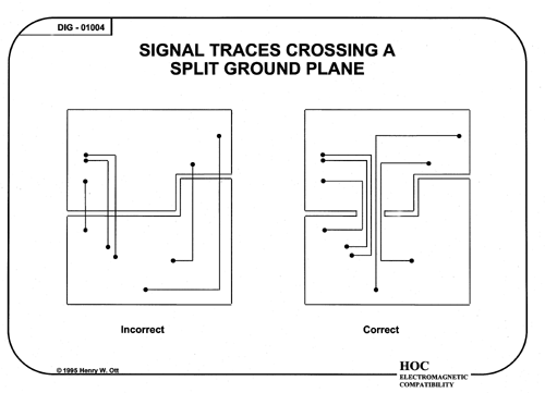
If you do split the ground plane and run traces across the split
(left
hand figure below), there will be no return path near the trace and the
current will have to flow in a big loop. Current flowing in big
loops
produce radiation and high ground inductance.
If
you must split the ground plane and run traces across the split,
you should do it as shown in the right hand figure below. By
connecting
the planes together at one point (a bridge) and routing all the traces
so that they cross at this bridge point, you will have provided a
return
path for the current directly underneath each of the traces (hence a
very
small loop area).
 High
frequency digital ground return currents want to return directly
underneath
the signal trace. This is the lowest impedance (lowest
inductance)
path. The digital ground currents have no desire to flow through
the analog portion of the ground plane and corrupt your analog
signal.
Why then do we need to split the ground to prevent the digital current
from doing something that it does not want to do anyhow?
Therefore,
I prefer the approach of using only one ground plane and partitioning
the PCB into digital and analog routing sections. Analog signals
can then be routed only in the analog section of the board (on
any
layer), and digital signals can be routed only in the digital
section
of the board (on any layer). What causes problems is when a
digital
signal is routed in the analog section of the board, or visa versa.
High
frequency digital ground return currents want to return directly
underneath
the signal trace. This is the lowest impedance (lowest
inductance)
path. The digital ground currents have no desire to flow through
the analog portion of the ground plane and corrupt your analog
signal.
Why then do we need to split the ground to prevent the digital current
from doing something that it does not want to do anyhow?
Therefore,
I prefer the approach of using only one ground plane and partitioning
the PCB into digital and analog routing sections. Analog signals
can then be routed only in the analog section of the board (on
any
layer), and digital signals can be routed only in the digital
section
of the board (on any layer). What causes problems is when a
digital
signal is routed in the analog section of the board, or visa versa.
A PCB with a single ground plane, partitioned
into
analog and digital sections, and discipline in routing
the signals can usually solve an otherwise difficult layout problem,
without
creating the additional problems caused by a split ground
plane.
If the layout is done properly, the digital ground currents will remain
in the digital section of the board and will not interfere with the
analog
signals. The routing, however, must be checked carefully to
assure
that the above mentioned routing restrictions are adhered to one
hundred percent! The key to a successful mixed
signal
PCB layout, therefore, is proper partitioning and routing
discipline,
not a split ground plane.
Many A/D converter manufacturers, while suggesting the use of split
ground planes, state the following in their data sheets or application
notes: "The AGND and DGND pins must be connected together
externally
to the same low impedance ground plane with minimum lead length.
Any extra external impedance in the DGND connection will couple more
digital
noise into the analog circuit through the stray capacitance internal to
the IC." Their recommendation is to connect both the AGND and the
DGND pins of the A/D converter to the analog ground plane. This
approach
has the potential of creating a number of additional problems.
Can
you list some of these problems? What do you connect the ground
side
of the digital power decoupling capacitor to? The analog plane or
the digital plane?
A much better way to satisfy the requirement of connecting AGND and
DGND pins together through a low impedance, and not create additional
problems
in the process, is to use only one ground plane to begin with.
The key to determining the optimum board layout is to think, how
and where do the return currents flow?
If you are still skeptical about using a single ground plane on your
mixed signal boards I suggest you do the following experiment.
Layout
the board with a split ground plane, but provide means for connecting
the
two planes together every 1/2 inch with jumpers or zero ohm
resistors.
Route the board properly, with no digital traces (on any layer) over
the
analog plane and no analog traces (on any layer) over the digital
plane.
Build the board and test it's functionality and EMC
performance.
Connect the planes together and test the board again for functionality
and EMC performance. I think that you will find that in almost
all
cases, both the functional performance and the EMC performance of the
board
will be better with the single ground plane. If you do the
experiment
send me an e-mail letting me know of your results.
It is almost always better to have only a single
reference
plane for a system!
Analog ground plane noise voltages should be kept smaller than the
minimum
analog signal level of concern. In the case of an A/D (or D/A)
converter
the smallest resolvable signal voltage level [least significant bit
(LSB)]
is a function of the number of the bits and the full scale reference
voltage
of the A/D converter. The smaller the reference voltage and the larger
the number of bits, the smaller the minimum resolvable signal voltage
will
be. The following table shows the resolution versus the number of bits
for an A/D converter using a one volt reference. These resolution
levels can be scaled for other reference voltages by multiplying the
resolution
by the appropriate factor. For example, if the converter uses a 5
volt reference then multiply the resolution numbers in the table by
five.
| Number of Bits |
Resolution (LSB) |
| 8 |
4 mV |
| 10 |
1 mV |
| 12 |
240 uV |
| 14 |
60 uV |
| 16 |
15 uV |
| 20 |
1 uV |
|
24
|
0.06 uV (60 nV)
|
The use of a single solid ground plane properly partitioned
and
routed (as discussed above) is usually adequate for most low to
moderate
resolution A/D converters (8, 10, or 12 bit). For higher
resolution
systems (14 bits and up) even more ground noise voltage isolation may
be
required for adequate performance. These converters have
resolution
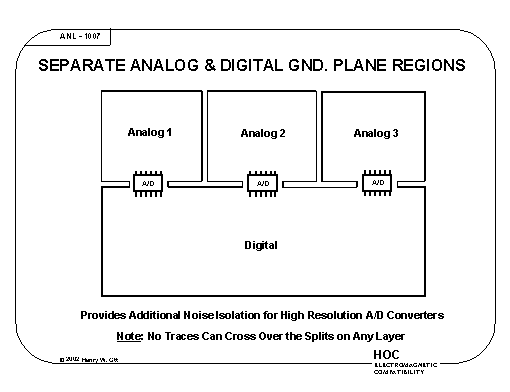
voltages in the tens of microvolts, or less, level. In this case
you might want to divide your board into separate isolated analog and
digital
ground plane regions, each solidly connected to the digital ground
plane
under each of the A/D converters as shown in the figure. This approach
will provide additional ground noise isolation for the high resolution
A/D converters while still maintaining a single ground plane for the
system.
Notice that even in this case, the ground plane is not split
--
it is all connected together. Also remember that no traces, on
any
layer, can cross over the isolating slots in the ground plane.
Summary
-
Partition your PCB with separate analog and digital
sections.
-
Do not split the ground plane. Use one solid
ground
plane under both analog and digital sections of the board.
-
Route digital signals only in the digital section of the board.
This
applies to all layers.
-
Route analog signals only in the analog section of the board.
This
applies to all layers.
-
The key to a successful PCB layout is the use of routing
discipline.
-
© 2000/2003 Henry W.
Ott
Henry Ott Consultants, 48 Baker Road Livingston,
NJ
07039 (973) 992-1793
Bibliography
Ott, H. W., Partitioning
and Layout of a Mixed Signal PCB, Printed Circuit
Design,
June 2001.
Correspondence
-
Thank you, this article will assist me in a proposal I made earlier
this
week in a design review on how to properly layout and partition a PCB
with
analog and digital signals. As you can probably imagine I was met
with major opposition when I proposed utilizing a bridge to connect the
analog and digital sections. I have used this technique on other
PCB's (different Business Unit) and had no problems although I never
had
the opportunity to conduct the experiment and analyze the data as you
mention
in your article, thank you very much. [e-mail from an engineer in
Michigan]
-
I am in the process of laying out a mixed-signal board myself and your
article has provided some useful information. Thinking of the
issue
in terms of return current flow makes a lot of sense. [e-mail from a RF
Engineer in California]
-
Your tech tip "Grounding of Mixed Signal PCBs" was the most clear and
concise
presentation of the material that I found. Everyone else suggest
separate planes connected at a single point but neglect to consider
"big
loops" as you suggest. Since you so clearly articulated (i.e., helped
me
understand the real issue), I am planning on purchasing your book
to hopefully better understand EMC design issues. [e-mail from an
engineer
in Arizona]
-
I am busy designing a mixed signal board incorporating two 16-bit DACs
and a high-speed digital side, and found your website very
enlightening.
It's amazing how much info there is out there by supposed "experts"
that
is clearly outdated or not very well thought through, and your website
provided a welcome change. [e-mail from a post-graduate student
in
South Africa]
Return to top of page.
Return to HOC home page.
Henry Ott Consultants
48 Baker Road Livingston, NJ 07039
Phone: 973-992-1793, FAX: 973-533-1442
March 25, 2004