Henry Ott Consultants
Electromagnetic Compatibility Consulting and Training
PCB Stack-Up
Part 6. Return Path Discontinuities
One of the keys in determining the optimum printed circuit board
layout is to understand how and where the signal return currents
actually
flow. Most designers only think about where the signal current
flows
(obviously on the signal trace), and ignore the path taken by the
return
current. Of course, the fact that many designers think this way
helps
to keep EMC engineers employed
To address the above concern we must understand how high-frequency
currents
flow in conductors. First, the lowest impedance return path
is
in a plane directly underneath the signal trace (irrespective of
whether
this is a power or ground plane) since this provides the lowest
inductance
path. This also produces the smallest current loop area
possible.
Secondly, due to the "skin effect," high frequency currents cannot
penetrate
a conductor, and therefore, at high-frequency all currents in
conductors
are surface currents. This affect will occur at all
frequencies
above 30 MHz for 1 oz. copper layers in a PCB. Therefore, a plane
in a PCB is really two conductors not one conductor. There will
be
a current on the top surface of the plane, and there can be a different
current or no current at all on the bottom surface of the plane.
A major EMC problem occurs when there are discontinuities in the
current
return path. These discontinuities cause the return current to
flow
in larger loops, which increases the radiation from the board as well
as
increases the crosstalk between adjacent traces and causes waveform
distortion.
In addition in constant impedance PCBs the return path discontinuity
will
change the characteristic impedance of the trace. The most common
return path discontinuities are discussed below.
Slots in Ground/Power Planes.
When a trace crosses a slot in the adjacent power or ground plane, the
return current is diverted from underneath the trace in order to go
around
the slot. This causes it to flow through a much bigger loop area.
The longer the slot the bigger the loop area becomes. The most
important
thing that I can say about slots in ground planes, is don't have
them!
If you do have slots, make sure that no traces cross over them on
adjacent
layers.
If you absolutely must route a signal across a power or ground plane
slot, place a few small stitching capacitors across the slot, one on
either
side of the trace (0.001 or 0.01 uF should be adequate). This
will
provide high-frequency continuity across the slot for the return
current.
To be effective the capacitors should be located within 0.1" of the
trace.
For more information on slots in power/ground planes see our Tech
Tip,
Slots
in Ground Planes.
Split Ground/Power Planes.
When a trace crosses a split in the adjacent plane, as in the 4-layer
board
example shown below, the return current path is interrupted. The
current must find another way to get across the split, which forces it
to flow in a much bigger loop.
__________________------------>_I_____________________Signal
Trace
_____I <--------------______
_____I_<------------____Split Power Plane
____________________I <------------____________________Solid
Ground Plane
___________________________________________________Signal
Trace
In the case shown above the current will divert to the nearest
decoupling
capacitor in order to cross over to the solid ground plane, then on the
other side of the split the current must find another decoupling
capacitor
in order to return to the power plane that is adjacent to the
trace.
The interplane capacitance between the power and ground plane is too
small
to be effective except in the case of frequencies considerably above
500
MHz.
The best solution to this problem is to avoid crossing split planes
with critical signal traces. In the case of the above example the
signal should have been routed on the bottom signal layer since that
was
adjacent to the solid ground plane.
If you absolutely must route the signal across the split plane,
place
a few small stitching capacitors across the split, one on either side
of
the trace. This will provide high-frequency continuity across the
split while maintaining dc isolation between the isolated sections of
the
split plane. The capacitors should be located within 0.1" of the
trace and have a value of 0.001 to 0.01 uF according to the frequency
of
the signal. This is far from an ideal solution, however, since
the
return current must now flow through a via, a trace, a mounting pad, a
capacitor, a mounting pad, a trace, and finally a via to the other
section
of the split plane. This adds considerable additional inductance
in the return path (5 to 10 nH minimum).
If in the above example both the power and ground planes are split,
you are really in trouble. I leave it to you to figure out how
the
current gets across the split plane boundary. In some instances
it
may have to go all the way back to the power supply. If you have
a split power and split ground plane the only acceptable solution may
be
to make sure that no signal traces cross the split plane boundary.
For additional information on split planes see our Tech Tip on Grounding
of Mixed Signal PCBs.
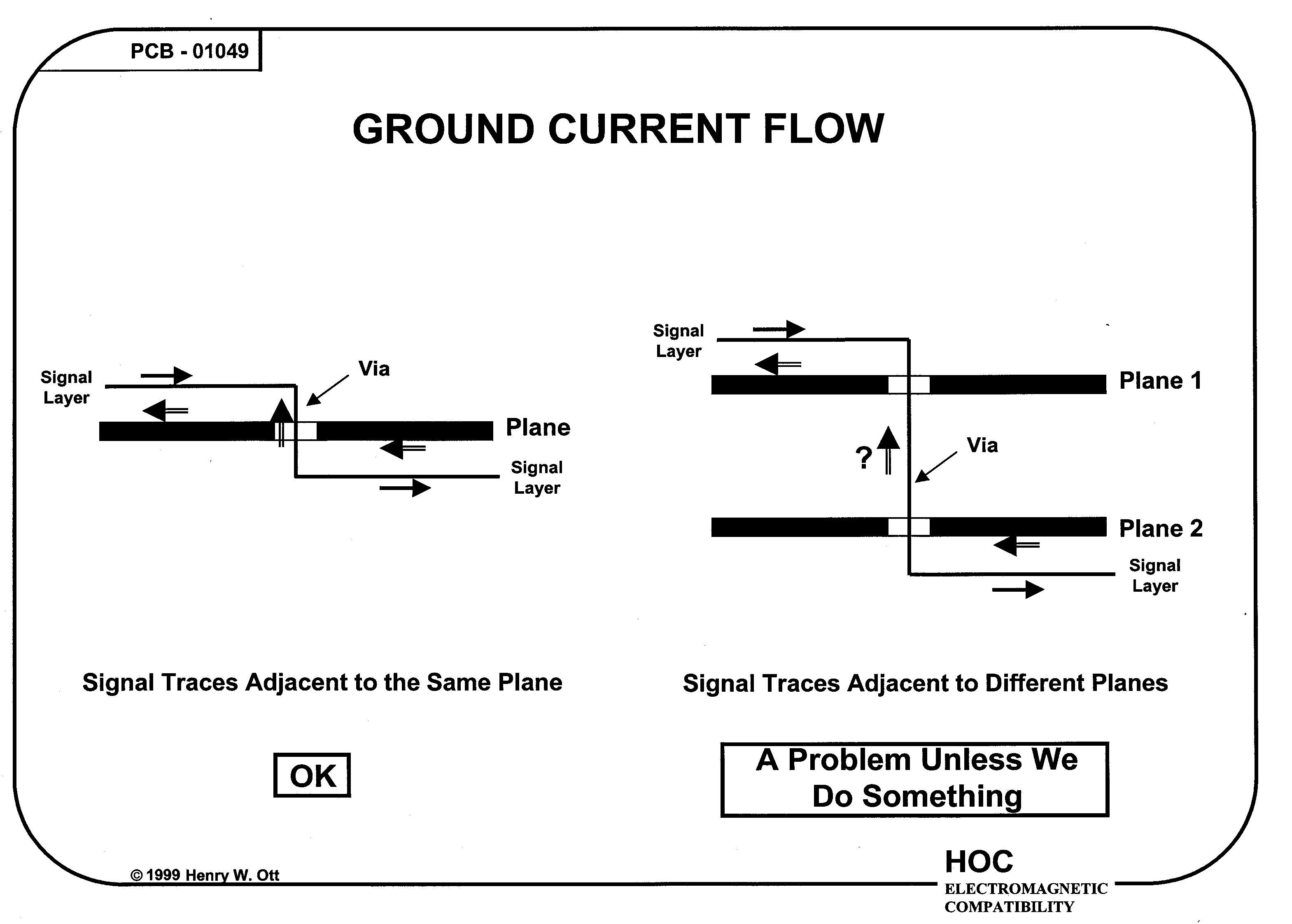
Changing
Reference Planes. When a signal trace changes
from
one layer to another on a PCB, the return current path is interrupted
since
the return current must also change reference planes (see right hand
figure
below). The question then becomes how does the return current get
from one plane to another? As was the case for the split planes
mentioned
above the interplane capacitance is not usually large enough to be
effective,
so the return current will have to flow through the nearest decoupling
capacitor in order to change planes. This obviously increases the
loop area and is undesirable for all the reasons previously
stated.
One solution to this problem is to avoid switching reference planes for
critical signals (such as clocks), if at all possible. If you
must
switch the return path from a power plane to a ground plane you should
place an additional decoupling capacitor adjacent to the signal via in
order to provide a high-frequency current path between the two planes
for
the signal return current. This is not an ideal solution,
however,
since the return current must now flow through a via, a trace, a
mounting
pad, a capacitor, a mounting pad, a trace, and finally a via to the
other
plane. This adds considerable additional inductance in the return
path (typically 5 to 10 nH).
Note, that if the two reference planes are of the same type
(either both power, or both ground) you can put a via (ground to ground
or power to power) instead of a capacitor immediately adjacent to the
signal
via. This is a much better solution than using a
capacitor
to connect the planes together, since the added inductance in the
return
path will be considerably less.
Referencing the Top and
Bottom
of the Same Plane. Whenever a signal switches
layers
and references first the top and then the bottom of the same plane we
must
still ask the question, how does the return current get from the top to
the bottom of the plane. Do to the "skin effect" the current
cannot
flow through the plane, it can only flow on the surface of the plane.
In order to drop a signal via through a plane a clearance hole must
be provided in the plane, otherwise the signal would be shorted to the
reference plane. The clearance hole provides a surface connecting
the top and bottom of the plane and provides a path for the return
current
to flow from the top to the bottom of the plane (see left hand
figure).
Therefore, when a signal passes through a via and continues on the
opposite
side of the same plane a return current discontinuity does not
exist.
This is, therefore, the preferred way to route a critical signal if two
routing layers must be used.
Summary.
High-Speed clocks and other critical traces should be routed (in order
of preference):
1. On only one layer adjacent to a plane.
2. On two layers that are adjacent to the same plane.
3. On two layers adjacent to two separate planes of the same type
(ground
or power) and connect the planes together with vias wherever the signal
changes planes.
4. On two layers adjacent to two separate planes of different types
(ground and power) and connect the planes together with capacitors
wherever
the signal changes reference planes.
Avoid routing clocks or other critical traces across slots or splits
in the adjacent plane. The above guidelines are important for all
PCBs carrying high-frequency signals, but are critically important in
the
case of boards with constant impedance transmission lines.
If you follow the guidelines presented in this series of articles,
with
respect to layer stack-up and the avoiding of return current
discontinuities,
you will produce better PCBs and avoid many of the most common EMC
problems
associated with boards. It will not guarantee you a perfect PCB
layout
but it will go a long way towards reducing the emission, increasing the
immunity, and improving the signal quality of your boards.
© 2002 Henry W.
Ott
Henry Ott Consultants, 48 Baker Road Livingston,
NJ
07039 (973) 992-1793
Return to top of page.
Return to HOC home page.
Henry Ott Consultants
48 Baker Road Livingston, NJ 07039
Phone: 973-992-1793, FAX: 973-533-1442
August 3, 2002