EMC Considerations in PCB Design and Layout
 This
one-day seminar covers Electromagnetic Compatibility (EMC) considerations
for digital printed circuit board design & layout. The seminar
is intended for PCB design and layout personnel as well as engineers interested
in PCB layout. Layout and routing techniques aimed at minimizing
both radiated and conducted emissions are discussed. Multilayer boards
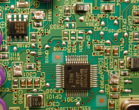
are emphasized. Topics covered include: clock routing, PCB
partitioning, decoupling, transmission lines, characteristics of ground
planes, and layer stack-up.
This
one-day seminar covers Electromagnetic Compatibility (EMC) considerations
for digital printed circuit board design & layout. The seminar
is intended for PCB design and layout personnel as well as engineers interested
in PCB layout. Layout and routing techniques aimed at minimizing
both radiated and conducted emissions are discussed. Multilayer boards
are emphasized. Topics covered include: clock routing, PCB
partitioning, decoupling, transmission lines, characteristics of ground
planes, and layer stack-up.
Outline
Introduction / Basic EMC Theory
Controlling Radiated Emission
---Common-Mode
---Differential-Mode
The PCB Review Process
Basic Principles of EMC
Skin Effect
Partitioning
---Component Placement
---Clock Location
---I/O Area
Board Routing
Clock Routing
Guard Traces
Crosstalk
Transmission Lines
---Microstrip
---Stripline
---Asymmetric Stripline
Decoupling Methods
Decoupling Problems
Use of Multiple Capacitors
Use of Distributed Capacitance
Capacitor Mounting
Power Plane Isolation
Ground Planes & Layer Stack Up
Characteristic of Ground Planes
Ground Plane Current Distribution
Slots in Ground/Power Planes
Layer Stack-Up Considerations
Examples of Typical Layer Stack-Ups
Return to top of page.
Return to HOC home page.
Henry Ott Consultants
48 Baker Road Livingston, NJ 07039
Phone: 973-992-1793, FAX: 973-533-1442
e-mail: h.ott@att.net
March 26, 2002